
Air plasma at atmospheric-pressure for improving conformal coating reliability
Mathieu Gonsolin. M. Sc.
EXELSIUS
Mouans Sartoux, PACA, France
ABSTRACT
Purpose:
Within many existing plasma technologies, air plasma at atmospheric-pressure remains one of the most commonly used in multiple industries. The implementation of air plasma at atmospheric-pressure is trendsetting in the conformal coating marketplace while low pressure plasma technologies are widely used for cleaning applications. This paper will review various plasma and gas systems and will explain how a newly developed cutting-edge blown air plasma at atmospheric-pressure process leads to the treated surface’s functionalization, transferring chemical energy for drastically increasing the conformal coating reliability while preserving boards’ integrity.
This paper will also review the suitability of blown air plasma at atmospheric-pressure to specific modern challenges of the conformal coating including de wetting defects and adhesion issues solving. Detailed examination of the effects of this blown air plasma at atmospheric pressure process on substrates will be presented based on numerous experiments, results and laboratory findings.
This paper will cover specific design configurations that allowed us to design and release an equipment to ensure the benefits of this patented plasma process, enabling flexibility, in line integration, automated programming, selectivity and reliability, known as the major expectations of the electronic
industry.
INTRODUCTION CONFORMAL COATING
Conformal coating is a protective chemical coating or polymer film 25-150μm thick (50μm typical) that ‘conforms’ to the circuit board topology. Its purpose is to protect electronic circuits from harsh environments that may contain moisture and or chemical contaminants. By being electrically insulating, it maintains long-term surface insulation resistance (SIR) levels and thus ensures the operational integrity of the assembly. It also provides a
barrier to air-borne contaminants from the operating environment, such as salt-spray, thus preventing corrosion.
The common failure in conformal coating includes cracking, dewetting, loss of adhesion, corrosion, poor capillarity flow, bubbles, foam. Surface properties of electronics devices, circuitry, uncleaned and contamination might result in failure in conformal coating.
Plasma technology, which is widely used for wire bonding, molding and underfill process can be used for surface activation of electronics boards, improving conformal coating adhesion, reducing drastically dewetting and delamination.
Let’s review plasma technology here first and examine that for a given plasma, used in a given condition, we can get the benefits without the risks for the industrial processing of electronic boards conformal coating.
OVERVIEW OF ATMOSPHERIC PLASMA
What is plasma?
The addition of energy into matter modifies electromagnetic forces, binding atoms together. The state of matter evolves from solid to liquid, then from liquid to gas. Adding even more energy dissociates molecular bonds and may lead to ionization. Gas molecules are split into charged particles, ions and free electrons.
Plasma is often called "the fourth state of matter".

Generating a plasma
Our partner’s plasmas are produced by electrical discharge through a gas. Firstly, gas is continuously injected into the plasma generator, then ionized and finally directed towards the surface to be treated.
Controlling the electrical discharge leads to a low temperature plasma coming out of the source. At high processing speeds, treated materials do not have enough time to increase their surface temperature. Heat-sensitive polymers are treated without damage.
Effects on surfaces
Plasma is a continuous supply of a highly reactive chemical species used for treating surfaces. Plasma can clean or activate surfaces.
Activation is the modification of the composition of a surface, resulting in a change of its surface energy. Surface wettability is drastically increased by grafting polar functions. Consequently, it can promote a stronger adhesion for paint, ink, glue or varnish. Plasma activation is a simple application, in a given and determined process window, that can allow a wide range of improvements.
Improving surface adhesion
Polymer surfaces have limited or no affinity with glues or inks. Poor adhesion means poor quality. Adhesion strength is definitively an important constraint in modern manufacturing.
Atmospheric pressure plasma processes tremendously increase adhesion strength. They can remove organic contamination from the surface and turn into an appropriate chemical preparation. Plasma treatment makes the strongest bond for industry requirements. Plasmas can increase tensile strength up to 10 times, and more. An optimized plasma treatment changes the failure of the adhesion joint from adhesive to cohesive.
Increase wettability, from hydrophobic to hydrophilic properties
Atmospheric pressure plasma processes increase surface energy of materials in two steps. Contaminants can be first removed and then, the plasma reacts with the surface, popping in appropriate chemical preparation that made it more hydrophilic. Glue, paint or ink will spread over surfaces easily. Atmospheric pressure plasma is a cost effective and efficient industrial process superseding harsh solvent methods which are no longer authorized.
Cleaning by oxidation of organic contamination, reduction of native oxides Surfaces are always contaminated by organic layers or native oxides.
This is often a consequence of storage or effects of previous processing steps. These contaminants need to be removed for functionality reasons or just to restore surface preparation before printing or gluing.
Thin oil films can be cleaned in a few seconds with an oxidizing plasma. Our partner plasma vendor is a clean and efficient alternative to mechanical and liquid cleaning processes.
Thin film deposition
CVD coatings (Chemical Vapor Deposition) are performed with atmospheric pressure plasma. Vapors of a suitable metal organic precursor are injected into the plasma. Uniform and homogeneous thin films can even be deposited on polymers.
Film deposition is a recent development topic and many applications for this technology are under investigation. Coatings give advanced functionalities to materials and are easily customized to customer specifications. For example, a glass film adds anti-abrasion property to a plastic part, anti-attrition property to metals or some new optical functionalities to glass.
Process engineers at the process development laboratory of our plasma vendor partner are currently studying these processes. Their support was a valuable resource for our company who wanted to benefit from these advanced processes.
We conducted numerous experiments and trials to finally, among a variety of atmospheric plasmas, select a special blown air plasma at atmospheric pressure for developing our cutting-edge plasma inline process solution, and let’s see now first the productivity we can get from it, and further how we assessed the associated risks of using this technology.
PRODUCTIVITY GIVEN BY OUR PLASMA SOLUTION
By increasing the surface tension, we can see easily the elimination of dewetting on populated boards.


Figure 1. Elimination of dewetting zones between plasma untreated and treated board samples


Figure 2. Comparison of Scarification test between plasma untreated and treated FR4 epoxy board samples

Figure 3. Positive effect of our plasma treatment on adhesion after thermal cycling
Adhesion measured according to IPC-TM-650 2.4.1.6 is given by scotch tape with force of 4N/cm2. These tests were done with different currently used coating material, acrylic, epoxy, polyurethane, silicone.
Independently from the coating we demonstrated that adhesion moves from class 0 to class 5, just by applying our plasma solution.
WHICH EXPERTISE CAN DRIVE TO SUCH A CUTTING-EDGE PROCESS SOLUTION?

Figure 4. Partners for implementing such a complex project
This project is not simply the use of a given plasma on a board. We worked with different partners to define the suitable plasma solution to use for inline series, the parameters to apply on the boards to achieve a given performance/effect and the corresponding hard and soft wares to process it.
For that we used computing science services, bonding engineering and plasma experts, and finally laboratories, pilot customer and huge skilled own resources to define and realize all tests and trials to be done for demonstrating the relevancy of our findings.
THEORY OF ADHESION, AND XPS ANALYSIS

Figure 5. Van der Waals Theory type London
We inquired on bonding theories and we concluded that our plasma relies on the chemically active free radicals diffused to the sample surface resulting in very high number of Van der Waals long distance, low energy bonds type London. These surface bonds with free radicals will balance with free radicals (H=Hydrogen) and COOR of the coating material, resulting in liquids and solids cohesion.
XPS, known as is X-ray Photoelectron spectroscopy, was used in Ultravacuum 2.10-7 mbar with a 200μm spot.
Samples used are epoxy with soldermask and other samples with NiAu finishing with RoHS deposit and Pb alloy deposits.

Figure 6. Comparison of surface oxygen rate given by our plasma treatment (XPS analysis)

Figure 7. Comparison of oxidized carbon bonds given by our plasma treatment (XPS analysis)
With our plasma solution, we demonstrated an increase of C-O, C=O and COOR oxidized bonds, as well as +5% average oxygen rate increase and +1% average Nitrogen rate increase.
All this was observed on an extreme surface within10nm to 15nm depth.
RISKS ANALYSIS, GENERAL APPROACH

Figure 8. Risk analysis on air plasma at atmospheric pressure applied on electronic boards
Based on our plasma solution, we conducted trials to understand the following risks: ESD, components functionality, thermal and physical impacts, ionic contamination, corrosion.
RISK ANALYSIS, CORROSION
Through the numerous treated components and boards, we observed the potential corrosion effect, and we have not ever seen any corrosion created by our plasma solutions.
RISK ANALYSIS, ESD
Our plasma solution forbids electrical current to leave the plasma nozzle, and then no electrostatic field can be applied on the boards, as well as no ionic contamination.
We apply our plasma on a field meter to test ESD.

Figure 9. ESD impact of plasma treatment given by Field meter measurement
Per IEC61340, the observed values are much below the minimum values, then our plasma solution doesn’t create any ESD effect.
Please see also illustration on quartz (Very ESD sensitive) measurement in the following section
RISK ANALYSIS, COMPONENTS FUNCTIONALITY

Figure 10. Functional tests on most commonly used electronic components
Based on our plasma solution, we conducted numerous trials to understand the risks on the functionality of the following components: Transistors and resistors, condensators and ferrite coils, LEDs, Quartz and diodes, integrated circuits and microcontrollers. All trials were done with minimum 10 of each component

Figure 11. List of tested components


Figure 12. Passed test resistance measurement impact of plasma treatment given by Ohm meter
Figure 13. Passed test capacitance measurement impact of plasma treatment given by LCR meter


Figure 14. Passed test of inductance measurement impact of plasma treatment given by LCR Meter
Figure 15. Passed test on frequency measurement impact of plasma treatment given by frequency meter and oscilloscope

Figure 16. Passed test on PWM Signal top time on 8-bit microcontroller
Our plasma solution does not change the functionality of the wide range of tested components, including the programming of microcontrollers.
RISK ANALYSIS, CYCLE TIME
There are different ways to use a plasma source. The main target of this solution was to define a solution that allows to make a fruitful plasma treatment in an inline process keeping the coating application process as the bottle neck.
RISK ANALYSIS, PHYSICAL IMPACT
We observed with both optical microscope and profilometer the surfaces with and without treatment


Figure 17. Absence of physical impact of our plasma treatment given by Optical microscope x50
Figure 18. Absence of physical impact of our plasma treatment given by Profilometer
Our plasma solution does not change the physical of the substrates.
RISK ANALYSIS, THERMAL
We measured with thermo couples the thermal effect due to the treatment with our plasma solution on an IPC test boards.


Figure 19. IPC Board treatment temperature measurement with 6 thermo couples

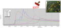
Figure 20. Example of plasma path, with different layers, on a populated board
Figure 21. Populated board temperature measurement with 6 thermo couples
The max temperature range measured is fully compatible with the standard boards processing temperature. We identified a risk due to the temperature ramp up given by our plasma solution, then, in addition to the functionality maintenance we already checked and demonstrated, made
some trials to measure the risk of component’s delamination, by acoustic microscopy which is the most advanced method for seeing this potential failure. We selected 11 types of components, sensitive to humidity, processed 1 or 2 reflow operations, and 1 or 2 of our plasma treatment, in standard parameters, and observed delamination at different stages, in the appropriated zones of the components.

Figure 22. List of components tested in acoustic microscopy


Figure 23. Acoustic microscopy versus X ray
Figure 24. OK or KO, what to observe in acoustic microscopy


Figure 25. Non-delamination of BGA 256 balls given by Acoustic microscopy analysis
Figure 26. Non-delamination of SOIC 20 pins given by
Acoustic microscopy analysis
Our plasma solution, though it transmits heat, does not impact the functionality and the reliability of the wide range of components we have tested, both separately and on assembled boards.
CONCLUSIONS
Our blown air plasma at atmospheric pressure solution, in line, in series, selective can overcome conformal coating adhesion challenges due to poor surface wettability. This study as a deep risk assessment shows that our plasma solution, bounding the process window, can increase the conformal coating reliability for the most populated coated boards, without affecting physical, chemical, functional, electrical performances.
By consequence, our plasma solution can enlarge the process window and open new opportunities, reduce the scrap level In addition, our inline selective plasma solution gives many advantages, over wet processing including:
- Environment benign process, no solvents, no waste
- Low cost of ownership & small footprint
- Excellent uniformity and reproducibility
- Low maintenance cost & ease of use
- X, Y, Z selective treatment, automated programming
- Can process different materials/substrates
This article was brought to you from the Proceedings of the SMTA South East Asia Technical Conference on Electronics Assembly 2017